I am a Senior Research Scientist at the University of Washington, broadly focusing on developing microscopy tools for analyzing complex materials for energy production and storage. I am currently “chief scientist” in the Ginger Lab where I am in charge of our atomic force microscopy (AFM) subgroup and associated research. I have ~19 years of scanning probe and optical microscopy expertise, from designing microwave probe methods to inventing entirely new analysis techniques. I have written many reviews, a book chapter, and I recently presented an extensive summary on this subject.
From 2012-2015, I was an “Optical Microscopy Tool Development Engineer” at Intel in Oregon, where I specialized in developing next-generation microscopy systems for failure analysis/fault isolation on the 14 nm and 10 nm nodes. My chief accomplishments include a patent on a visible light probing system for subsurface semiconductor analysis that was licensed, near-field scanning optical microscopy of an active processor test chip, and using super-resolution microscopy to improve optical debug. I received a company-wide award for using structured illumination to image an actively-functioning test chip. I also helped develop electron microscopy tools for non-destructive analysis of processors.

At UW, I currently focus on microscopy as relating to:
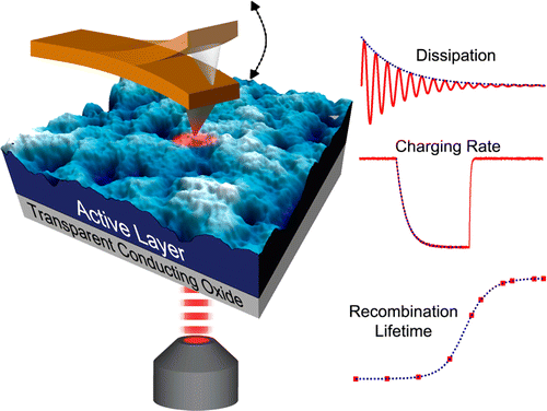
- Photovoltaics: I am studying perovskite solar cells using novel AFM methods with an emphasis on “big data” microscopy analysis. I am particularly interested in measuring how these materials can be improved by analyzing how they respond to light at the nanoscale. An example is using the AFM to measure how quickly charge is generated as a function of how polycrystalline the material happens to be. More recently, I have been using AFM to show
- Biosensors and Neuromorphic Computing Devices: I am studying how conducting polymers can be used in cutting-edge applications, largely in neuromorphic computing devices as well as biosensors, depending on the material. These materials use ions (charged atoms) to reversibly dope the film, and are known as “mixed conductors.” This research includes a high-profile demonstration using AFM to directly image how nanoscale structure impacts ion transport. These studies are naturally related to battery and energy storage as those are ion conductors, but my personal interest is in memristive applications such as hardware-based neural networks and memory-based computing.
- Data-driven analysis of microscopy: I’m broadly interested in how we can use more advanced microscopy analysis to understand our materials. I spearheaded the Ginger Lab’s first foray into this field back in 2012, using signal processing of time-resolved microscopy data to enable resolution at fractions of a cantilever cycle. Among other things, I’m an active contributor of the Pycroscopy and PyUSID packages and am the primary developer of our lab’s main microscopy analysis package, fast free transient analysis. Much of this work resulted in recent work investigating a simple neural network for analyzing highly complex microscopy data.
For more information, here is my current CV. You can also check out my publications, or just go to my Google Scholar page.
I received my B.S in Electrical Engineering from UT-Austin, where I was a National Merit scholar and a Cockrell scholar, and I graduated with high honors in 2004. I then received my M.S. and Ph.D. at Rice University working for Prof. Kevin F. Kelly in 2007 and 2009, respectively. I focused on scanning tunneling microscopy of polymer nanowires. While in graduate school I was the fortunate recipient of an NSF Graduate Research Fellowship and several University-wide awards. I was then a post-doc at the University of Washington before spending several years at Intel.
I’m always interested in new ideas or discussions, particularly as they relate to new ideas in microscopy and image processing! Please contact me either via LinkedIn (links on this page) or via e-mail (from my CV).